NSOM Probes
Near-field scanning optical microscopy (NSOM) is a technique can achieve spatial resolution performance beyond the classical diffraction limit by employing a sub-wavelength light source or detector positioned in close proximity to a specimen. Such a sub-wavelength source usually consists of an aperture at the end of a tapered probe, which functions basically as a wave guide.
In transmission-mode NSOM, light is coupled to the waveguide from an external source (such as a laser) and directed through the tip of the probe. The ideal probe is one in which the incoming electromagnetic radiation passes through only the very tip of the probe. A single-mode optical fiber is the most commonly utilized type of probe for near-field microscopy, and can be fabricated with either a straight or curved (bent) tip. Bent optical fiber probes are normally operated in tapping-mode feedback, while the straight optical fiber probes are operated in shear-force mode feedback.
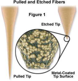
There are two primary physical requirements for high quality near-field probes. The first is that the tip should terminate in a well-defined aperture of sub-wavelength size. Secondly, the probe shape must allow access to the specimens of interest. The original concept for a near-field scanning optical microscope, as proposed by Edward H. Synge, consisted of a sub-wavelength aperture in a conduction screen that would be scanned over an extremely flat object. In practice, if specimens were chosen or modified to have flat planar surfaces, appropriate apertures could be fabricated in suitable materials using electron-beam lithography. Unfortunately, most specimens that are the subject of microscopic investigation do not have perfectly flat surfaces. Hence, the majority of the probes fabricated for employment in NSOM techniques are macroscopically tapered to a sub-wavelength aperture, which allows the aperture to be scanned in close proximity to surface features of varying height. Figure 1 illustrates optical fiber probe tips with tapered regions created by pulling and by etching techniques. Currently applied tip fabrication protocols can produce dramatically different taper geometry, surface characteristics, and optical properties.
Fiber Probe Fabrication
NSOM probes have been fabricated from a variety of materials, including cleaved crystals, atomic force microscope (AFM) cantilever tips, semiconductor structures, glass pipettes, and tapered optical fibers. Following creation of the tapered tip, the sides of the probe are coated with an opaque metal film (usually aluminum) to prevent light loss in regions of the waveguide other than the aperture. The very tip of the probe is left uncoated and this transparent region defines the aperture of the probe. Some of the first macroscopic light guides were fabricated by pulling heated glass micropipettes, but now the majority of probes are created from single-mode optical fibers. When compared with metal-coated glass pipettes, single-mode optical fibers have more than 1000 times better collection and transmission efficiency. Single-mode fibers deliver the maximum amount of light to the apex of the tip (where the aperture is located), as compared to multi-mode optical fibers.
Physical limitations restrict the minimum aperture diameter that can be created utilizing current techniques. The two primary constraints on aperture size include:
- Metal film coatings applied to the probes have a finite skin depth (the minimum thickness required to produce opacity), which limits the minimum probe size that can be coated with sufficient thickness to prevent penetration of light through the walls of the tip.
- The metal coating used on the probes is generally produced by thermal evaporation and exhibits a structural graininess. The grain size restricts approach of the tip to the specimen, and may affect the symmetry of the aperture itself. Mathematical modeling of factors involved in producing metallized probes has estimated the minimum diameter for a probe aperture to be approximately 10 nanometers (for light of 514-nanometer wavelength).
The first stage of NSOM probe fabrication is tapering of the single-mode fiber down to a fine tip. There are a variety of techniques that have proven useful for fiber tapering, but the task is most commonly accomplished by heating and pulling or by chemical etching, and in some cases both methods are combined to create the desired taper characteristics.
Pulling Method
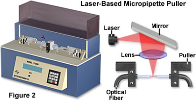
A popular technique for producing a tapered fiber tip relies on carefully controlled heating and pulling of a single-mode optical fiber until the point of rupture. This is accomplished with the most reliability by utilization of a commercial micropipette puller (as illustrated in Figure 2). These devices are commonly used for creating tapered pipettes for biological uses, such as patch clamp experiments, and nucleus transferal, and function by locally heating the glass (with a laser or heating coils) to a temperature of approximately 1600 degrees Celsius and then applying a reproducible tensile force to the fiber. The fiber breaks at the point of heating, creating two tapered fibers having very fine points at the rupture location. Once the heating and pulling parameters are optimized, the desired taper and tip diameter can be produced with high reproducibility, a major advantage of the pipette puller technique.
Although tips can be reliably produced by pulling micropipettes, a disadvantage of the technique is that the taper is usually much longer than on tips produced by certain other methods (see left-hand image in Figure 1). Probes with a longer, more gradual taper typically have lower transmission efficiencies than those with shorter tapered regions, for a given tip aperture diameter. Typical aperture diameters of NSOM probes produced by the pulling method range from approximately 50 to 100 nanometers.
Meniscus Etching
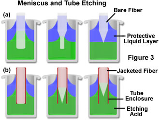
An alternative method of taper formation, which allows greater control of the cone angle produced on the optical fiber, utilizes a powerful etchant such as buffered hydrofluoric acid. In this technique, termed meniscus etching (patented by Dennis R. Turner in the 1980s), the etchant is typically covered by a protective layer of a hydrophobic chemical such as toluene or p-xylene that serves to form a meniscus along the fiber tip during etching, as well as to prevent corrosion of the optic fiber above the tip region by the etchant vapor (see Figure 3). Etching occurs at the point where the meniscus is formed along the fiber as it is dipped into the layered fluids. The properties of the protecting layer determine the shape and contact angle of the meniscus formed, and therefore the choice of this substance determines the cone angle that is produced at the fiber tip. The meniscus etching method produces a much shorter taper (approximately one-third in length) compared to the pulling method, as illustrated in Figure 1. Cone angles up to 41 degrees, and a variety of novel probe configurations, have been reported in studies using meniscus etching. The large cone-angle tips provide at least an order of magnitude higher optical efficiency, as well as better preservation of polarization properties, in comparison to pulled tips.
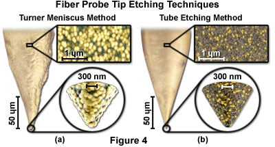
The main drawback of the meniscus etching technique is that the tip shape and its surface quality are quite sensitive to the etching environment. Air movement, temperature fluctuations, vibrations, and etchant concentration can have a strong influence on the shape and symmetry of the meniscus-etched probe, and on its surface roughness (note the surface of the tip illustrated in Figure 4(a)). If the surface of the tip is too rough or is marred by other imperfections, then the subsequently applied metal coating can have pinholes that interfere with the definition of a near-field aperture. Irregularities can also become starting points for thermal degradation of the metal coating, thereby lowering the fiber damage threshold and reducing its useful lifetime.
Selective Etching
Another variation of chemical etching that overcomes, to some extent, the environmental sensitivity of meniscus etching is referred to as selective etching or tube etching. The selective etching process takes advantage of the different etching rates exhibited between the core material and the cladding surrounding an optical fiber. Rather than removing the polymer jacket from the fiber prior to etching (as illustrated in Figure 3(a)), the cladded fiber end is immersed in the etchant, which usually consists of a buffered hydrofluoric acid solution (Figure 3(b)). Because the fiber jacket is resistant to degradation by the etching solution, the entire etching process takes place inside the hollow tube formed by the jacket, as the fiber itself is reduced to a tapered geometry. One advantage attributed to tube etching over conventional meniscus etching is the extremely smooth glass surface and taper shape that is produced, probably due to the protective environment of the tube enclosure. Note the differences in surface roughness of the tips produced by the Turner meniscus method (Figure 4(a)), and the tube etching method (Figure 4(b)). The tube etching process is apparently self-limiting, in that no further tip deterioration occurs if etching is continued after the tip formation is complete.
In general, chemical etching techniques are preferred over the pulling method because the resulting probes have a sharper taper angle, and correspondingly higher optical transmission efficiencies (up to three orders of magnitude higher). The selective etching technique normally results in a sharpened-pencil shape, but multiple etch procedures can produce multiple taper angles and increased transmission and collection efficiencies. One significant disadvantage of the chemical etching technique is the very hazardous chemicals (such as hydrofluoric acid) that are required for the etching process.
Apertureless and Alternative Probe Designs
A number of other probe designs have been considered by investigators, and some implemented, to overcome the limitations of standard fiber optic tips. Many of these can be categorized among a group referred to as apertureless probes, and hold significant potential for improving the spatial resolution of near-field microscopy techniques. One of the probe design concepts employs standard non-metallized silicon nitride AFM tips. These tips convert nonpropagating radiation in the near-field into a measurable far-field signal in a photon tunneling configuration. In addition, non-metallized optical fiber probes have also been used in the photon tunneling scheme. This is similar in concept to total internal reflection fluorescence (TIRF) imaging, except that instead of fluorescent molecules receiving the evanescent excitation, the uncoated probe collects this near-field energy.
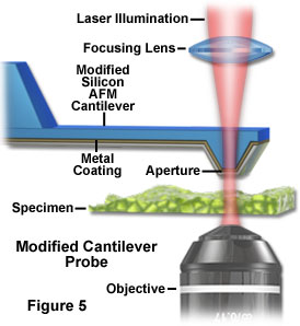
Micromachining and photolithography techniques have enabled fabrication of NSOM silicon nitride and silicon cantilevers, which are similar to atomic force microscopy cantilevered probes with the exception of an added aperture. Figure 5 illustrates a silicon AFM cantilever probe modified to deliver near-field illumination through an aperture at the tip, while operating in force-feedback mode. The atomic force signal and collected optical information can provide simultaneous topographic and high-resolution optical images. Typically the aperture modification is made by coating the transparent silicon cantilever with an opaque aluminum layer, followed by creation of a sub-wavelength-sized aperture in the aluminum at the tip by milling with a focused ion beam. The illuminating radiation is coupled into the tip by focusing a laser beam onto the probe.
Another tip design variation involves the use of small amounts of luminescent or fluorescent material placed at the very tip of a capillary probe. Excitation of the material, followed by migration of light emitting excitons to the tip end, produces a miniature light source at the probe tip that can be scanned over the specimen surface. Many challenges must be overcome before this type of probe becomes a feasible alternative to the fiber optic probes. One of these problems is the development of reliable fabrication methods that allow control of tip geometry. Another is the photobleaching of the luminescent probe material, which can greatly decrease the useful lifetime of this type of probe.
A method similar to the one described above combines attributes from both NSOM and fluorescence resonance energy transfer (FRET) techniques. The basis of the technique is to attach the acceptor chromophore (dye) of a FRET dye pair to the tip of an uncoated NSOM probe. Light passing through the NSOM probe, which is nonresonant with the acceptor dye, excites the donor dye that is present in the specimen. As the tip scans over regions of the specimen that contain the donor dye, energy is transferred from the excited donor to the acceptors bound to the NSOM tip. These acceptors then produce a red-shifted fluorescence signal. Recently, investigators have reported utilizing fluorescein and rhodamine as the donor/acceptor pair to obtain FRET images of a Langmuir-Blodgett film at sub-diffraction spatial resolution. As is the case for the exciton tips, photobleaching of the fluorescent dyes remains a significant problem with this technique.
Metallic Probe Coatings
Metallized optical fiber probe tips are currently the most common type of NSOM probe. The quality of NSOM images is largely governed by the light-transmitting aperture defined at the probe tip by the metallic coating. As the diameter of an uncoated fiber in the taper region is reduced beyond the mode-field cutoff of the fiber waveguide, light escapes from the sides of the probe tip, compromising the characteristics of a well-defined aperture. Thus, a critical parameter in most NSOM probe fabrication procedures is the application of an opaque metal coating to reduce light loss through the tapered region of the fiber, and to confine its emission to the desired aperture. For the visible region of the electromagnetic spectrum, aluminum has the smallest skin depth and thus, in theory, should allow for the minimum effective coating thickness on the probe sides.
In practice, the performance of deposited aluminum coatings is compromised by the tendency of the metal to form grains, and thicker coatings (than would be predicted from the theoretical skin depth) are required to prevent light leakage. To compensate for the leakage resulting from granularity, a coating thickness of 50 to 100 nanometers is usually applied around the taper region of the probe. The texture of the aluminum coating produced by vacuum evaporation is represented in the tip enlargement in Figure 1. Other metals, including silver, chromium, and platinum in combination with carbon, have also been used successfully as probe coating materials, although aluminum is the most common.
Vacuum Evaporation
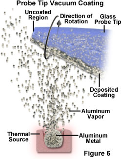
Coating of NSOM tips is usually accomplished by vacuum evaporation. Although sputtering techniques have advantages in many applications, certain characteristics of the evaporation process make it generally preferable for deposition of aluminum on probe tips. The directionality of deposition during thermal evaporation (in contrast to the scattering at multiple angles that is characteristic of sputtering) is advantageous because line-of-sight deposition allows the aperture region of the probe to be easily shielded from the metal vapor. This is accomplished by simply orienting the probe so that the tip is directed away from the evaporation source, and rotating it in such a way that the sides are evenly coated, while the aperture region at the tip remains uncoated (see Figure 6). The technique of shielding the apex of the probe tip from the evaporating metal in order to produce an aperture for the passage of near-field light was first applied to pulled micropipettes and later adapted to optical fiber probes.
A further advantage of evaporation over sputtering techniques for aluminum deposition is the much higher speed, which minimizes the formation of oxides on the metal surface. Oxides of aluminum form very rapidly on freshly deposited surfaces, and adversely affect the surface smoothness and reflectivity, both of which are critical parameters in the performance of near-field probe tips. The steps that are customarily taken to reduce grain size in evaporated films are all beneficial in improving the smoothness and reflectivity of probe coatings. These include increasing the coating rate, reducing the total vacuum chamber pressure, and reducing the partial pressures of water, oxygen, and hydrocarbons in the chamber.
Plasma Coating
Sputtering of metal, utilizing a plasma discharge, is an alternative to thermal evaporation for coating the sides of near-field microscopy probes. The deposition of metal by plasma sputtering is a multi-directional process, and it is commonly employed in many applications that benefit from its characteristic of uniform deposition on irregular surfaces. As a consequence of this behavior, plasma sputtering of NSOM probes results in the entire tip being coated, and an aperture must be created in a subsequent process. An opening in the metal can be produced by lateral contact between the tip and a surface, for example by scanning the tip over a hard surface with a large applied force (low feedback set point voltage). Apertures as small as 20 nanometers in diameter have been created in this manner, although generally the aperture becomes larger after several hours of use, probably due to the heating of the tip (resulting from photon absorption).
Although plasma coating is a simpler method than evaporation for applying metal to probes, and it is generally accepted that sputtered metal films are of higher quality than those produced by evaporation, the performance of the resulting tips has typically been much lower. Reproducibility of the aperture is a significant problem, as is the degrading oxide formation (discussed previously) that is favored by the relatively slow sputtering process.
Focused Ion Beam Milling
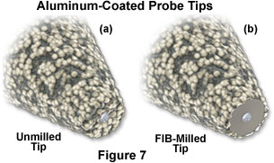
A technique of micro-milling the tip aperture utilizing a focused ion beam (FIB) has recently become popular, and offers a promising approach to improving the aperture characteristics of metal coated tips, much as the various novel methods of probe taper formation have been applied toward improving overall tip geometry. A focused ion beam is capable of producing or altering structures on a nanometer scale, and allows precise modifications to be made to the geometry of a near-field probe tip. The aperture area of an aluminum-coated probe exhibits relatively large metal grains that not only significantly extend the dimensions of the probe itself, but also may alter the shape and symmetry of the aperture (see Unmilled Tip illustration, Figure 7(a)). By physically restricting the close approach of the tip to the specimen, the grains limit the resolution achieved and the photon intensity, which in term decreases signal-to-noise ratio. The imperfections in aperture symmetry can introduce various optical aberrations and cause modification to polarization characteristics of the light passing through the tip.
The focused ion beam instrument can be employed to precisely remove the very tip of the probe, producing a remarkably smooth and flat surface, surrounding a highly symmetrical aperture (Figure 7(b), FIB-Milled Tip). The removal of coarse grain structure at the probe tip enables it to be positioned in much closer proximity to the specimen surface. Dramatically improved performance has been observed utilizing FIB-modified tips, compared to unmodified versions, with some single molecule fluorescence measurements showing an intensity improvement of an order of magnitude. Additionally, increases in polarization extinction ratios have been measured, typically ranging over 250 to 1.
Among the drawbacks of FIB milling are the high cost and limited availability of the necessary equipment, the additional time required in milling the tips, and the failure rate associated with fabricating tips in this manner. In addition, the absence of aluminum grains at the tip of a milled probe has a negative effect on the force imaging characteristics in NSOM. These grains, or perhaps a single grain at the aperture, generally act as a stylus in the interaction between specimen and tip, and determine the quality of force images. Consequently, for NSOM applications that require simultaneous collection of optical and high-resolution topographical information, FIB-milled probes may not be the optimum choice.
Maximum NSOM Probe Throughput
The optical throughput efficiency (and power output) of a metal-coated probe is strongly dependent on physical parameters specific to the particular probe tip. Light loss occurs as the diameter of the tip in the taper region is reduced below the cutoff between propagating and near-field (evanescent) light waves. Because a portion of the light that is lost is absorbed in the metal coating of the probe tip, the maximum light throughput is effectively limited by the localized heating that occurs at the tip of the probe, due to the photon absorption. Local heating damages the coating, and in most cases the tip aperture, either through direct thermal effects, or as a result of stresses caused by the different thermal expansion coefficients of the glass and metal. Both calculated and experimentally measured temperature profiles show heating to exhibit a strong dependence on the taper angle of the tip, increasing with decreasing taper angle. The lower efficiency and greater thermal damage in longer pulled fiber tips is one factor limiting their use in low-signal applications.
In certain NSOM operational modes and applications, the amount of light coupled into the fiber is sufficient to produce significant localized heating, and various mechanisms have been employed to minimize the associated problems. It has been experimentally determined that the application of a protective coating (such as chromium) on the probe tip prior to aluminum coating, or the deposition of alternating titanium and aluminum layers, yields probes that are more robust. These mixed coatings prevent degradation due to both mechanical wear and laser heating. The optical destruction threshold of probes coated in this manner has been shown to increase approximately 400 percent, as compared to conventionally fabricated probes coated only with aluminum.
Following fabrication and metal coating, probe tips may be characterized by scanning electron microscope (SEM) and optical microscope examination. The electron microscope provides much better resolution than optical methods, which is beneficial in evaluating the grain size and texture of the evaporated metal. However, optical microscopy has the advantage of revealing pinholes or other light transmission anomalies along the length of the probe that might produce spurious results during imaging. This type of evaluation is not readily achieved with electron microscopy.
Ultimate NSOM Resolution Limit
The fundamental resolution limit of NSOM is governed by four parameters:
- Skin depth of the metal coating.
- The grain size of the metal coating.
- The probe aperture diameter.
- Inherent noise in the optical signal and electronics.
The skin depth of a coating layer is determined by the finite penetration of optical waves into the metal, which is typically a few nanometers. The grain size of the probe coating determines how closely the tip can approach the specimen, and is also a primary factor affecting the size of spaces between grains, through which light leakage can occur. The number of transmitted photons varies in relation to the fourth power of the NSOM probe aperture diameter.
All of the resolution parameters listed above ultimately play a role in determining the signal-to-noise ratio of the image information. The smaller the probe aperture, the lower the light transmission through the probe tip. In addition, reduction of transmission through the tip taper region leading up to the aperture limits the power output through the probe. This power loss reduces the signal-to-noise ratio and is the limiting factor in realizing the ultimate resolution in many near-field applications. Published calculations of power within the tapered region of a probe of typical geometry, as a function of distance from the aperture, indicate a reduction in transmission of nearly nine orders of magnitude as the diameter of the fiber tapers from 100 nanometers to 20 nanometers. The inefficiency of the tips is a result of the transition from propagating waves to evanescent waves as the diameter of the taper region decreases, and light is either reflected back up the fiber from the taper region or absorbed by the metallized coating at the tip. The lost light results in a smaller signal, and hence, a lower signal-to-noise ratio.
Currently, the optical and mechanical properties of fiber-based probes are still rather poor and remain as the limiting performance factor for many NSOM applications. A number of researchers have suggested that with increased development and utilization of FIB milling techniques, it may be possible to fabricate probe tip structures that function as waveguides to eliminate the mode cutoff. This has yet to be practically demonstrated, although a wide array of NSOM applications would benefit from increased transmission efficiency and output from fiber optic probes, including single-molecule spectroscopy, Raman spectroscopy, data storage, and high-speed imaging. Although many companies commercially produce NSOM probes, current fabrication processes are not suitable for large-scale production. Each probe must still be individually inspected for pinholes and other flaws. Therefore, optical fiber-based NSOM probes remain relatively expensive, and the cost is likely to remain high until more efficient probe fabrication techniques are developed.
