Channel Photomultipliers
Channel photomultipliers represent a new design that incorporates a unique detector having a semitransparent photocathode deposited onto the inner surface of the entrance window. Photoelectrons released by the photocathode enter a narrow and curved semiconductive channel that is illustrated in the tutorial figure. Each time an electron impacts the inner wall of the channel, multiple secondary electrons are emitted.
These ejected photoelectrons have trajectories angled at the next bend in the channel wall (simulating a dynode chain), which in turn emits a larger quantity of electrons angled at the next bend in the channel. The effect occurs repeatedly, leading to an avalanche effect, with a gain exceeding 100 million. The tutorial initializes with a single photon impacting the photocathode and producing a corresponding photoelectron, which then moves through the curved channel chain. Use the Stop button to start and stop photon flow, and the Gain slider to control the number of photoelectrons produced by the channel. The photoelectrons flow through the channel and eventually are captured by the anode. When the Stop button is activated, photoelectron flow through the channel tube ceases.
The spectral response, quantum efficiency, sensitivity, and dark current of a photomultiplier tube are determined by the composition of the photocathode. The best photocathodes capable of responding to visible light are less than 30 percent quantum efficient, meaning that 70 percent of the photons impacting on the photocathode do not produce a photoelectron and are therefore not detected. Photocathode thickness is an important variable that must be monitored to ensure the proper response from absorbed photons. If the photocathode is too thick, more photons will be absorbed but fewer electrons will be emitted from the back surface. However, if the photocathode is too thin, too many photons will pass through without being absorbed.
The channel photomultiplier illustrated in this tutorial is a revolutionary design that eliminates the hundreds of elements necessary to construct a conventional dynode chain. Advantages of this design are lower dark current (picoamp range) and an increase in dynamic range.

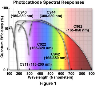
A wide spectrum of photocathode/window combinations are available with the channel photomultiplier to allow use of the device over a wide range of spectral responses (from 115 to 850 nanometers; see Figure 1). The most appropriate combination for optical microscopy is the C944, which operates with high quantum efficiency over the visible wavelength range of 300 to 650 nanometers.

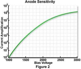
Unlike many older model photomultipliers, the channel photomultiplier requires only a single high voltage supply without the need for an external voltage divider network. At a maximum bias voltage of 3000 volts, anode gain can exceed 100 million (Figure 2), with a sensitivity of 3 million amps/watt at a wavelength of 410 nanometers using a bialkali photocathode. This performance exceeds that displayed by conventional photomultipliers and avalanche photodiodes by several orders of magnitude. When equipped with specialized photocathode/window combinations, the channel photomultiplier is also a very efficient photon counter.
